16GB iPod Nano 3G Upgrade
2026-09-05
Watch the first video
I first had this project idea in April of 2020 at the beginning of the pandemic. I didn't really know how long it would be (the project or the pandemic) and I was curious why nobody had tried this before (the project, not the pandemic). At this point, I had no soldering experience, no reverse engineering experience, and while I'd been working with software at some level since I was five years old, to this point I had very little hardware experience outside of working with Arduinos at a very "Adafruit" maker level. I didn't realize how big of a challenge this would be, mainly because I was learning everything from scratch. But now that it's done, I can confidently say that it was worth it. It took longer than it should have, but give me a break.
An Introduction To The Problem
You've probably seen some videos on YouTube of people upgrading the storage in their iPod Classics, pushing it to 1TB, 2TB, and 4TB (whereupon it fails, since it runs out of RAM to handle that many songs). While I wouldn't call the hard drive in the large iPods "user serviceable", it certainly is compared to the NAND chips found in iPod Nanos, Shuffles, and everything else Apple makes now (with the exception of AirTags, I guess). I naively thought that swapping out the NAND chip in a Nano would be easy and it would simply Just Work™.
I chose the iPod Nano 3rd Generation for two reasons. First, it's the newest revision of the Nano that has a NAND chip with legs (which was less out-of-my-league than BGA soldering but still out-of-my-league). Second, it's the Nano closest to my heart because it's the one I had growing up. I loved that thing. People loved their iPods - proven by the popularity of some Australian drummer and snake owner's YouTube channel about iPods that isn't actually about iPods because there is only so much content you can make about iPods.
Taking apart any Nano is hell. It's possibly impossible to do it without destroying it. But, if you manage to get into the 3rd Generation Nano (which I will be referring to as the 'n3g' from here on out), you immediately see the NAND chip.
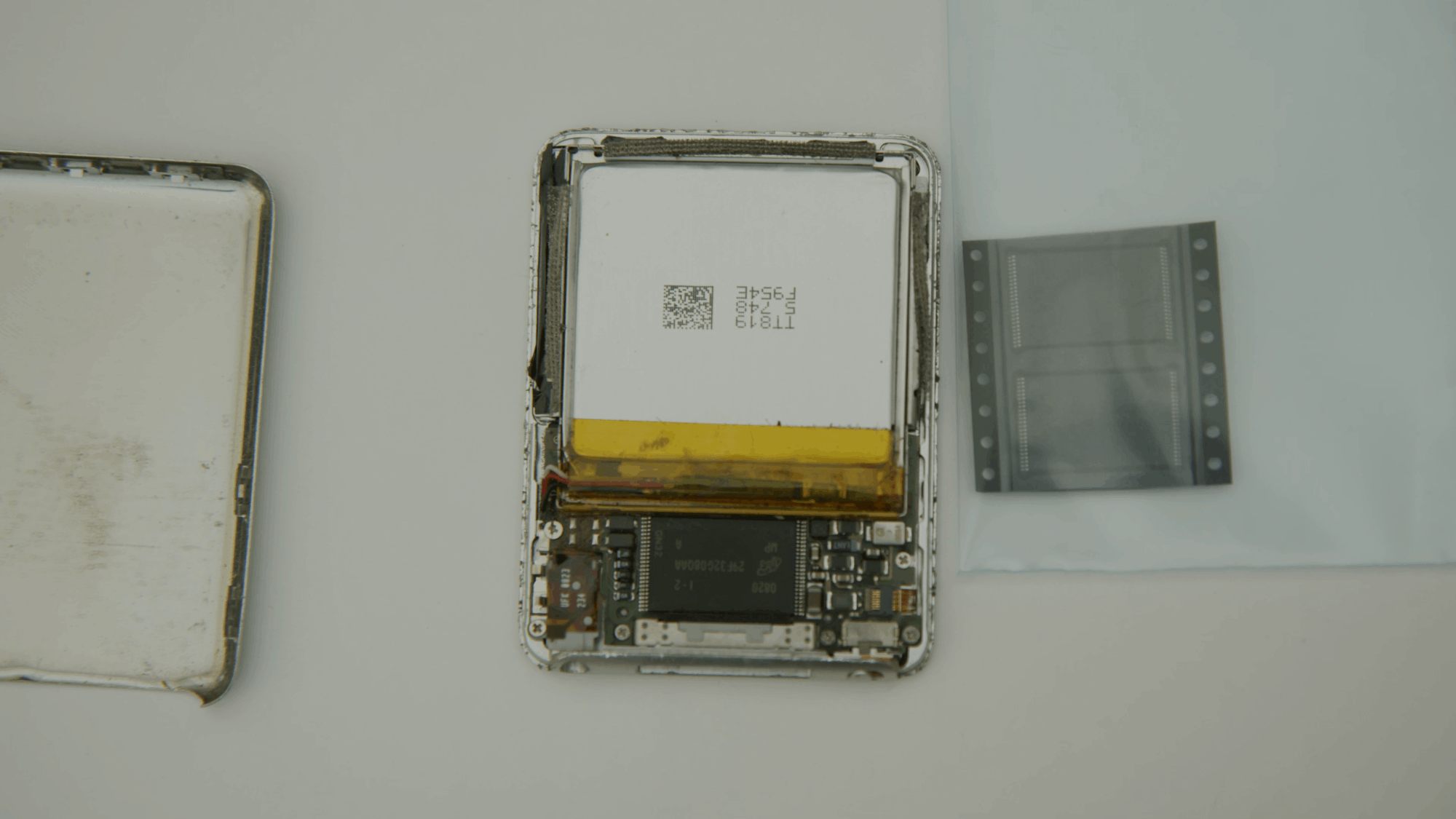
Desoldering it is easy enough with low speed hot air. Soldering it is less easy. The first few iPods were done by my good friend Wesley in his garage.
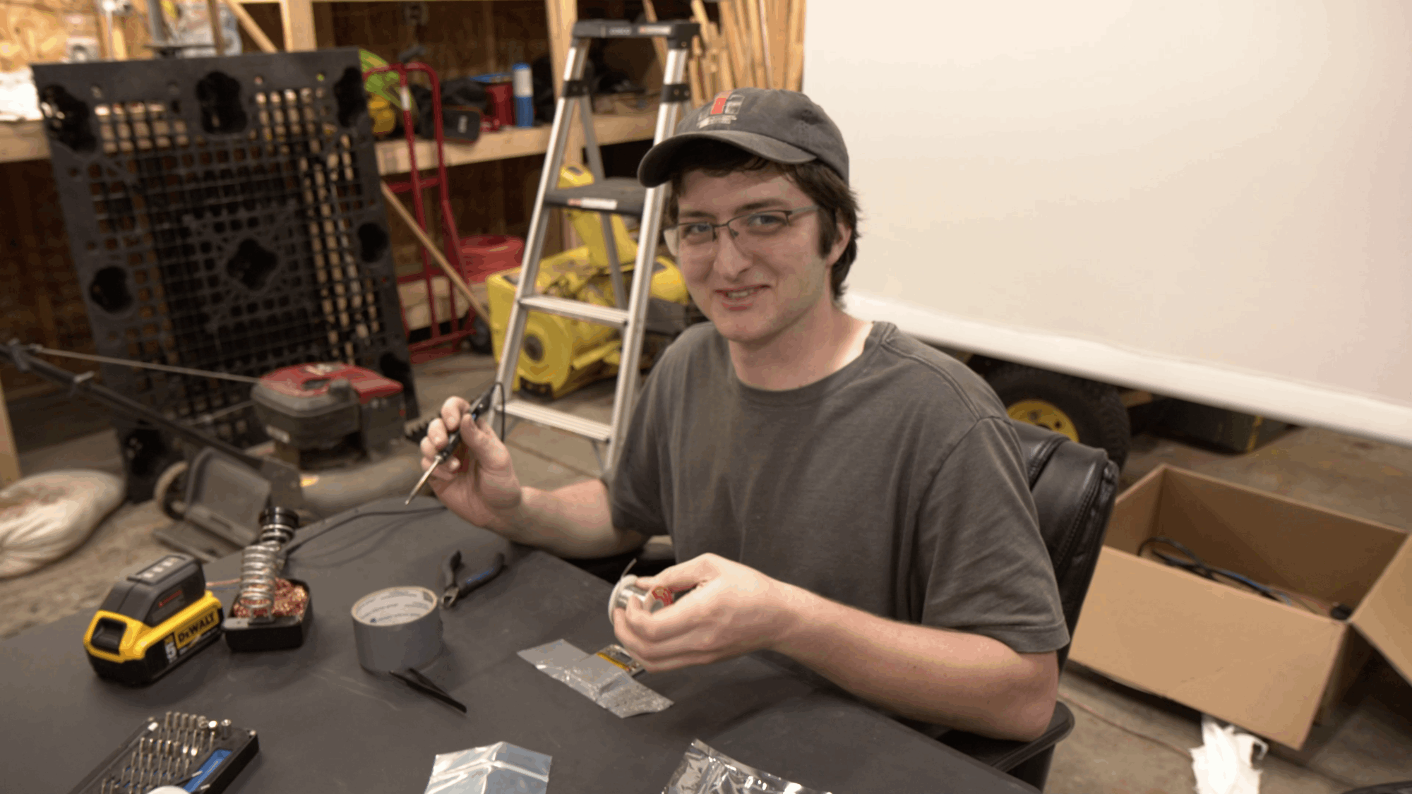
"This is it," I foolishly thought as I held the camera waiting to see that blessed 16GB in the "About" section of the iPod UI. But no. What we got instead was the dreaded Red X.

The Red X
Standing in Wesley's garage, I thought this meant "this chip is unformatted, where's my operating system?" which made sense to me. I tried recovering the iPod and found that iTunes couldn't even see it. Wesley has experience in embedded electronics, and explained that usually there's some sort of table of acceptable NAND in the firmware and, if the chip isn't found in that table, it just stops. I went back home determined to figure out what was going on and mod my way into getting this thing to work. How hard could it be? I just have to find the table and patch it out with the details of the NAND chip, right?
My first discovery confirmed Wesley was right. I found a similar table in Rockbox's n2g port:
struct nand_device_info_type
{
    uint32_t id;
    uint16_t blocks;
    uint16_t userblocks;
    uint16_t pagesperblock;
    uint8_t blocksizeexponent;
    uint8_t tunk1;
    uint8_t twp;
    uint8_t tunk2;
    uint8_t tunk3;
} __attribute__((packed));

static const struct nand_device_info_type nand_deviceinfotable[] =
{
    {0x1580F1EC, 1024, 968, 0x40, 6, 2, 1, 2, 1},
    {0x1580DAEC, 2048, 1936, 0x40, 6, 2, 1, 2, 1},
    {0x15C1DAEC, 2048, 1936, 0x40, 6, 2, 1, 2, 1},
    {0x1510DCEC, 4096, 3872, 0x40, 6, 2, 1, 2, 1},
    {0x95C1DCEC, 4096, 3872, 0x40, 6, 2, 1, 2, 1},
    ...and a lot more...
};
This table had to come from somewhere, obviously, so I needed to find where the n3g's version was in its firmware. It turns out an almost identical table shows up in several places across the n3g firmware. After doing some research and talking to some people in the Rockbox IRC channels, I inherited some half-done reverse engineering work from some developers who, years prior, were trying to port Rockbox to the n3g. This included the Rockbox bootloader and led to my very first success in getting code to run on the iPod. I knew code execution would be the first real hurdle, and the fact that someone had already done this was a huge step in the right direction.
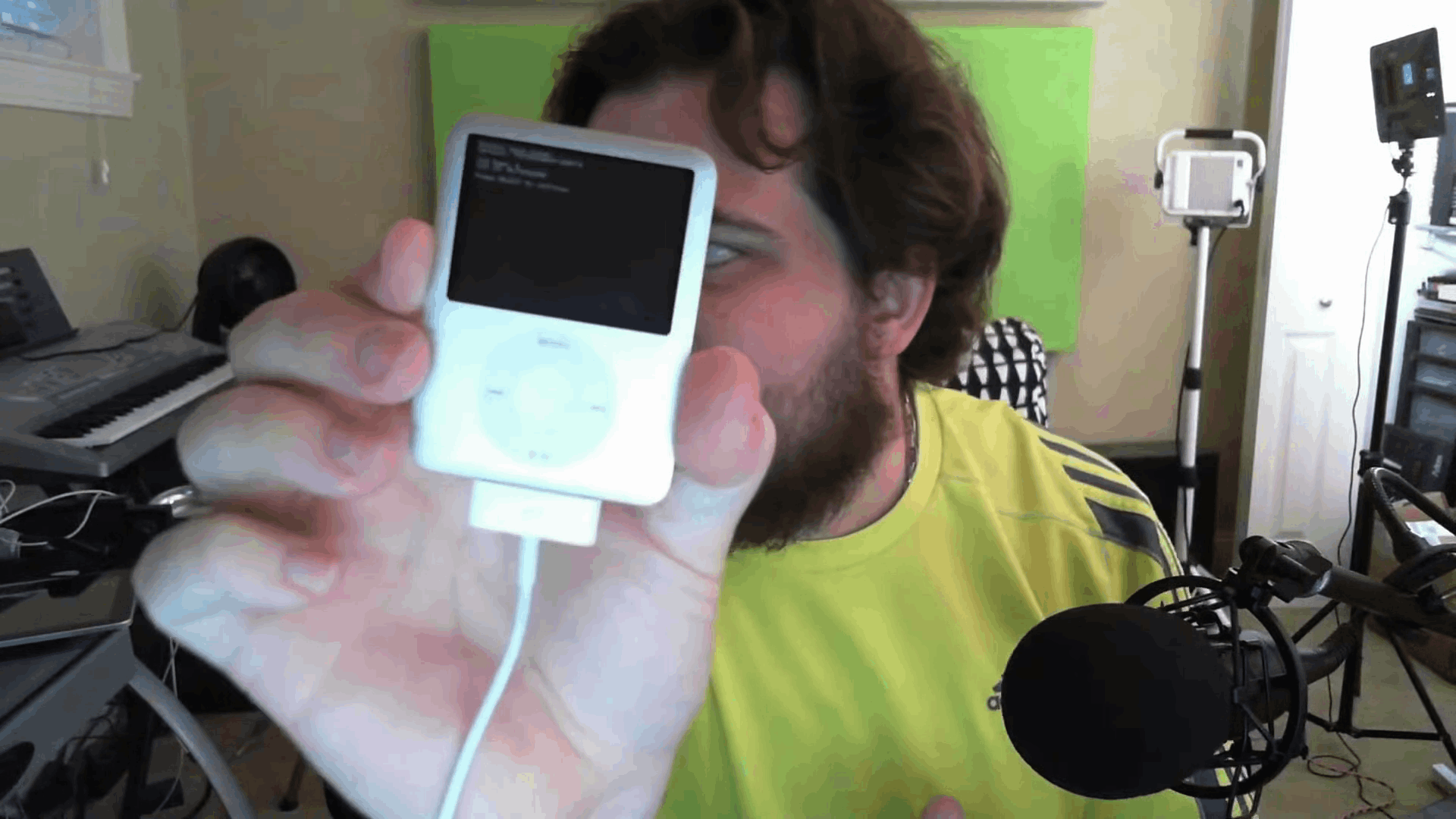
The Rockbox bootloader uses the Pwnage 2.0 exploit to run code. You can read more about it here and here, but it's basically a stack-overflow exploit targeting a bug in the ASN.1/DER certificate parsing logic of early Apple S5L8xxx BootROMs. Because the entire certificate chain parsing context (der::chain::parse_ctx) is allocated on the stack, and the saved link register (LR) sits at a known offset just past the end of that structure, an attacker can craft a malicious last certificate whose oversized signatureValue overflows the buffer by 344-345 bytes, overwriting the saved LR with an attacker-controlled address. The attacker can place arbitrary executable shellcode there, and the overwritten return address simply redirects execution to that payload, achieving full unsigned code execution at the BootROM level. Once you can run code, you can see and dump code.
The first piece of the firmware we have to touch is what I refer to as the EFI bootloader because that's exactly what it is. I was sort of shocked when I saw this - I always thought EFI (and UEFI, but don't expect Apple to do anything U) was primarily for computer bootloaders. I guess Apple was full-steam-ahead on EFI in the Apple TV, Macs, and who knows what else, so it makes sense. Still, it felt heavy for something like this and, what's more, it made static analysis somewhat harder.
The NAND table in the EFI exists in the NAND driver. I know, shocking, but we can follow the codepath to the spot that identifies the chip ID and from there I found the NAND driver's initialization routine. Basically, during initialization, the NAND driver checks the IDs of the banks of NAND, initializes some buffer memory, the VFL, the FTL, and then opens both of them. It was obviously breaking at step 1, so I swapped out the ID and geometry in the table for the chip that I had.
In the early days, my patching methodology was very annoying. The Rockbox bootloader was capable of reading and writing from NOR flash. Every time I wanted to try a patch out, I had to follow these horrible steps:
- In a hex editor, write the patches I want to try by changing bytes. Save it.
- Using UEFITool, replace the NAND driver PE32 binary with mine. Save it.
- Run it through a binary diff algorithm I made for this purpose but it's probably not very efficient.
- Compile that into the Rockbox bootloader.
- Upload and run the Rockbox Bootloader which loads the EFI from NOR and unpacks the diff's bitstream on top of it, then writes the modified EFI back to NOR.
- The bootloader then boots NOR and I watch for my patch.
This process was horribly manual and not very fun. To further complicate things, I was keeping track of my patches in an Excel spreadsheet. Pain.
Changing the NAND Table's parameters didn't help. I was still getting the dreaded Red X. That image is called bdhw in NOR. Bad hardware. So it still wasn't happy. I wasn't sure why. I needed some sort of introspection. The EFI really doesn't export anything user-visible. The image it shows, I guess (bdhw, bdsw, lbat, etc.), but that's not coming from within the NAND module. So I had two tools up my sleeve.
Tool 1: Spinning
This one is barely worth a paragraph so I'll be brief: I was able to bisect code paths by adding a b . at one branch of a conditional to see if the iPod froze or not. Very cool, very standard. Nothing special about that.
Tool 2: Exfiltrating Data Through The Diagnostic Mode
This one is more interesting. At first, I thought the EFI had no sort of output, it just loaded everything up, showed a boot splash, and then jumped to the binary it was supposed to load. Early on, I figured the answer to "how does the iPod know about its NAND" could be easily found in diagnostic mode's NAND LBA field. But when I looked into it, it seemed to be reading the value from somewhere magical. It would find something in memory - "sysI" - and grab a value at an offset and show it. Diagnostic mode does not deal with NAND itself. So it must be getting passed that information from somewhere, right?
After some more investigation, I discovered that I was looking at the System Information Table. The EFI builds this across several modules and passes it along to the binary it loads. The table includes everything from SysCfg (like serial number, model number, etc.), RAM information, and crucially the NAND LBA count. This part of the table gets created in the NAND driver's entry point after driver initialization. The initialization code returns the calculated NAND LBA count, but what if we bubbled something else up out of there. We're not actually initializing NAND, so maybe we can smuggle some data out of there, four bytes at a time?
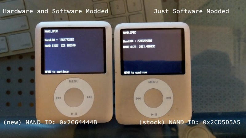
NAND_SPEC test.Through a series of patches, this is what I did. The proof of concept for this patch was to smuggle out the NAND ID. That's what's shown in the picture above. This proved that the iPod was actually able to communicate successfully with the NAND chip. Through a combination of Tool 1 (conditional spin-lock) and Tool 2, I was able to find why at this point the NAND driver was failing to initialize.
Why The Driver Was Failing To Initialize
When the iPod comes across a virgin NAND chip, it tries to "production format" it. This involves setting up VFL and FTL structures. This part was failing, and I wasn't sure why. I bisected my way through the production formatting path and found that it ended up in a failed memcmp within a function that writes the very first VFL structures. It erases the block, writes the structure (in this case, a driver signature), and reads it back to verify that it made it to NAND. The failing memcmp causes it to retry a few times before giving up and returning failure, halting the format, boot, and resulting in bdhw.
Through smuggling data out four bytes at a time through NAND_SPEC, I found why it was failing: the verification read was all FF as if the chip hadn't been written. At this point, it was unclear if the entire write was failing or just the first four bytes, but it made the most sense that the entire write was failing. But why?
The FMISS Layer
This is a little bit of an aside because at this point I went down a massive rabbit hole that truly helped me understand the NAND peripheral and how it actually works with the NAND chip itself. I was expecting to see reads and writes to a NAND peripheral with addresses, commands, all sorts of stuff. Instead, what I saw was something passing a binary blob and a bunch of parameters and saying "go". So, what is this?
I'm not sure what it's actually called. I've seen it called FMISS, I've seen it called FIL, I've seen it called CS (code sequencer). It might be all of these, it might be none of these. It's a coprocessor that runs bespoke bytecode (or microcode? not sure on definitions here) that offloads the act of interacting with NAND. It's not used in any other way and it's in the same address space as the direct FMC itself so it's definitely intended to be used with NAND. Either way, it has its own ISA and figuring out what it did was probably the most satisfying part of this whole project (besides getting the final product to work).
You can read about the exact instruction set here, but I think it's more prudent here to talk about how I actually figured out how it works. I think I just made the right number of leaps to get to a mostly-working understanding of everything.
My ground truth was a leaked data sheet of the S5L8700X which is an older chip closer to one found in an n2g. I pored over the NAND section and found no such reference to FMISS or a state machine or anything like that. But what I did find were register definitions (outdated but somewhat helpful) and step-by-step sequences for how developers should write NAND functions. I was really beating my head against the wall for a while asking myself "how does the iPod write commands to the NAND chip?" For example, the READ ID command - 0x90 - never shows up in the ARM code. So it must live in the bytecode, right?
It does. By looking at the Read ID program and the Read Page program, I was able to find those command bytes and I also found there were four bytes preceding it each time. This revelation showed me the basic structure of the bytecode. It was clear that each "instruction" is 64 bits and organized in a weird endianness. I wrote a small C program to just printf the instructions it knew about so I could fill in the gaps with parts of the process that made sense.
It was basically objdump for this bytecode. At first, almost every instruction was "unknown" but as I cross-referenced with the "how do you NAND?" instructions in the datasheet, I was able to pull apart more instructions. The register map was also somewhat helpful because I could tell where in the sequence I was and how much more to expect. I'm particularly proud of how I discovered branching and jumps in the bytecode because loops are heavily used in these programs.
At some point, I was modifying the firmware to confirm my guesses. I replaced the Read ID microcode with my own and saw the results in the NAND_SPEC test results. I was able to write an assembler and disassembler for the bytecode (nothing fancy, just smart enough to produce readable code, I guess). I got about 90% of the way to a complete documentation of this state machine's instruction set. q3k corrected some of the finer points, and together we wrote the FMISS emulation into QEMU. More on that later.
The good news is also the bad news: this had nothing to do with my problem. Understanding the FMISS layer may have been important in an indirect way, but I probably could have completed this project without ever going down this path. That said, I think it was worth it just for that: I'm not sure I'll ever get another excuse to reverse engineer an undocumented instruction set. It was quite satisfying.
This is where the first video I posted ended. Check the scroll bar, we have a long way to go.
Waves
With that digression out of the way, I was now stuck with only one way forward: what's actually happening on the NAND bus? Is there some weird thing happening that this chip doesn't support? I tried to go about this in numerous ways, but the only thing that gave me a reliable signal capture was using a data recovery spider board:
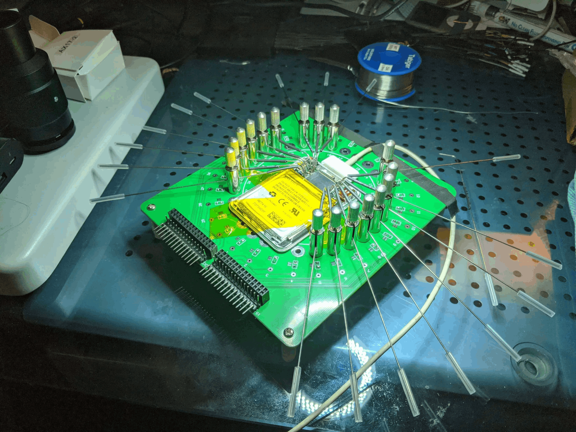
I attached this to a DSLogic U3Pro32 and started looking at what was actually occurring over the wire. And what I found was disappointing but not surprising:
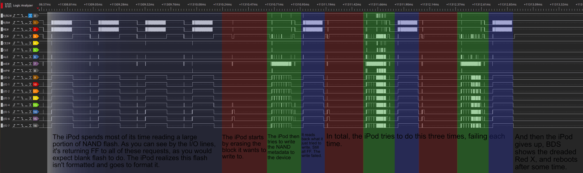
Not surprising because this is exactly what the code says it does, disappointing because I'm not sure why it's doing it. The NAND is outright rejecting page programs. That's odd. I traced through the signals to see if it was issuing strange read/write commands and no, they're your standard commands. It's almost as if the chip is write protected or something.
Is the chip write protected?
Unbelievably, the WP# leg on the NAND was not attached to the pad. It wiggled like a loose tooth. So I soldered it down and, of course, it got further. But not that much further. It's able to write and verify until, like, page six. Okay, now what?
Just a Bit More
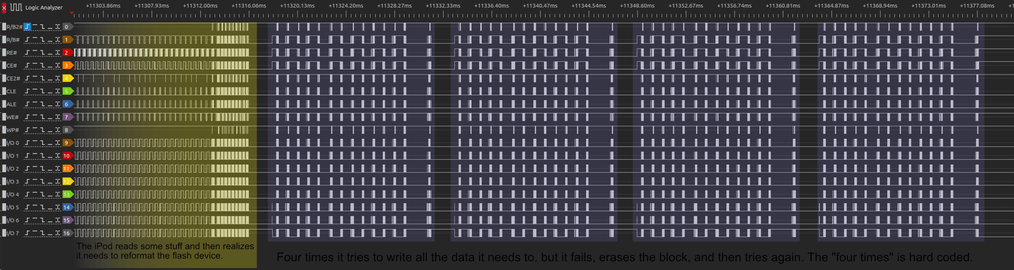
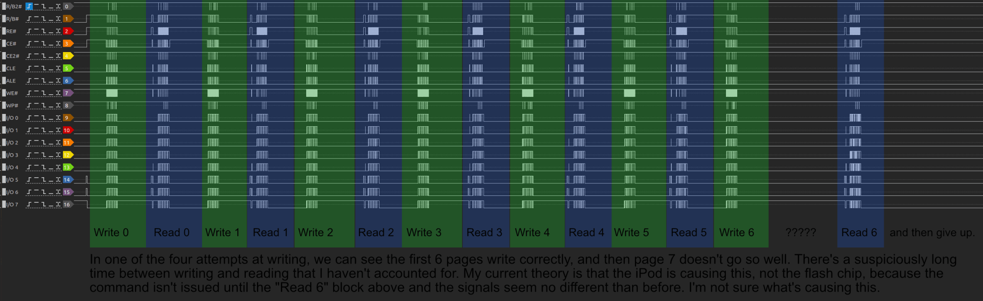
The first six pages were writing beautifully. But then we hit page six and, much like the publication, it was useless and full of noise. I know NAND is prone to bitflips but this was bad.
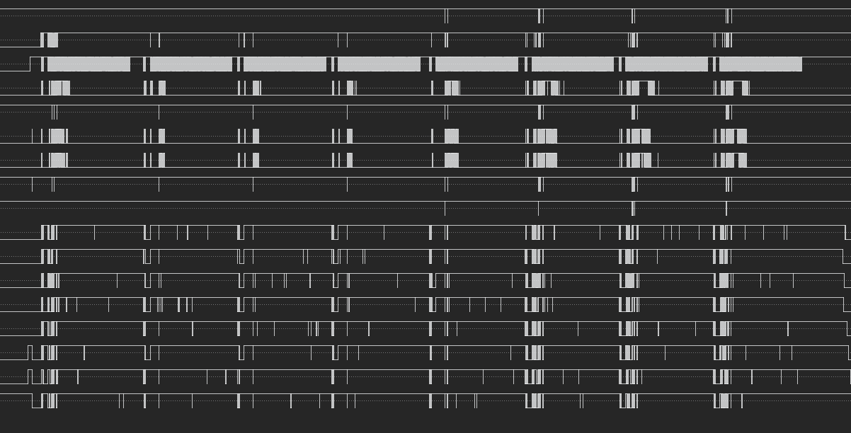
I also replicated this behavior across a few of the same chips. Is this an insane number of bitflips? I didn't know then, but I know now: this is not an insane number of bit-flips for MLC NAND. But why does this pattern start on Page 6?
This confusing and unrelenting pattern led to my first burnout when I turned my attention to adding fully digital Bluetooth to the n3g. But, as always, I crawled back to this project for more pain.
My friend, Cooper, used to work for one of the big NAND manufacturers and gave me his manager's email address. His manager explained exactly what was happening and why. NAND stores data as trapped charge across a huge array of cells. In Single Level Cell NAND, each cell holds one bit: an empty cell reads as a 1, a charged cell reads as a 0. Fresh from the factory every cell is empty, so every bit is a 1. "Programming" selectively pushes charge into cells to turn them into 0s, and the only way back to 1 is erasing the whole block.
Multi Level Cell (MLC) NAND is the next step. Throwing more cells at the density problem gets expensive - the physical device grows large and complicated - so instead we pack two bits into a single cell. Define four voltage levels, assign each a two-bit value, and now one cell holds two bits.
You might already see the problem here: with four levels crammed into the same range, the margin for a misread shrinks. The first bit is easy to decide - its margin is wide - while the second bit is far tighter. That's the trade-off behind MLC, TLC, QLC, and beyond: you need smarter error correction to handle the bitflips and the tighter margins, but the chips stay "cheap" while storing enormous amounts of data.
That explains the noise, but not the pattern. The two bits in a shared cell don't belong to the same page - they're the nth bit of two different pages, and the datasheet tells you which pages are paired. On this chip, pages 0 and 6 share cells. The easy first bit goes to page 0, so it reads clean. Page 6 rides on the tight second bit, so it comes back noisy.
This left me with two choices. I could either figure out how to beef up the error correction calculations done on the iPod, or spend the money and get the expensive SLC chip. I opted to kick the ECC can down the road and swapped the chip on a fresh iPod with a 16GB SLC chip and of course it worked. The EFI was able to format the chip successfully and we made it to disk mode!
So that's it, right? I just have to patch disk mode in the same way and I get a 16GB iPod Flash Drive! No. No, that's not what happened. Disk Mode is complicated. It's basically a stripped down version of the iPod's full operating system - both are based on a real-time operating system called RTXC. So it was back to the drawing board to figure out what was going on.
The iPod speaks SCSI over USB, and the SCSI "READ CAPACITY" command returns the number of blocks and the size of the blocks for the device. Disk mode's capacity math works out how many logical blocks the device has by dividing the logical block size by the NAND page size and scaling by the page count. On every chip Apple ever used in the n3g, that ratio is a sensible whole number - a 4096-byte page gives 1, a 2048-byte page gives 2. On an 8192-byte page like the new NAND has, it computes 4096 / 8192 = 0. That zero then lands in two different places, each failing differently. The page converter multiplies by it, so every request becomes "zero pages." And the capacity math divides by it, which faults outright - a data abort, a panic, a reset, and a boot loop.
So I patched it to calculate the ratio off of 8192 without really knowing what it did because that's the change that made the crash stop. With that, the device came up but it never mounted anything. I heard the "something is plugged in" Windows chime (don't worry, I was developing in a Linux VM) but it never went beyond that. So I looked to dmesg and found:
sd 2:0:0:0: Attached scsi generic sg0 type 0
sd 2:0:0:0: [sda] Unsupported sector size 8192.
sd 2:0:0:0: [sda] 0 512-byte logical blocks: (0 B/0 B)
sd 2:0:0:0: [sda] 8192-byte physical blocks
This one stumped me for a good, long time. It led to my second burnout, wherein I focused my efforts on QEMU and other rehosting projects for the iPod, and also repurposing the iPad 3rd Generation into a touch screen you can plug in and use with any computer. I have a strange way of stepping away from projects.
Rehosting
I want to digress again and talk about my rehosting efforts since they pay off later in the story. There are two avenues I pursued basically in parallel:
Full Emulation
I thought it would be cool and useful to get an iPod fully emulated. That way I could get some dynamic analysis and stop with the painful bisection methods above.
My first emulator used the Unicorn Engine. It was able to make it all the way through the BootROM (so SPI and GPIO were basically working) and most of the EFI, but it was hilariously slow because it was emulating every instruction one by one. Then devos50 published his QEMU fork emulating the first-gen iPhone, so I forked it and went in. I knew QEMU was the right choice from the start but it was a bit intimidating to start from scratch implementing, well… everything, because I wasn't sure how to write QEMU code. Seeing the diff between his work and the base he forked from gave me confidence that I could do it too, so I dove in. And it was doing pretty well. Big breakthroughs at first were the I2C peripheral, the hardware JPEG decoder, and the FMISS instruction set in the NAND peripheral.
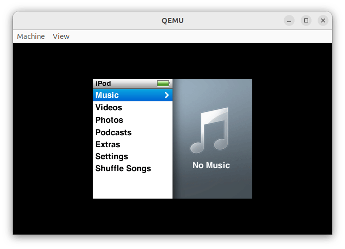
Later, a member from the iPod Nano Discord server named Iscle forked a more modern QEMU version to build an iPod Classic emulator. We're working on emulating the same chip, and his project layout didn't inherit the strange organization of devos50's fork, so I ported my nano-specific work over. I pushed it further and it now boots disk mode and RetailOS and enumerates over USB/IP, so you get a virtual iPod virtually attached to your machine. There are still a massive number of things that don't or will never work, but for the 16GB project, it's basically sufficient. It certainly helped with the below efforts. Here's that project.
User Space Emulation
Perhaps a more novel approach to dynamic analysis was just running the NAND driver in Linux Userland. I thought of several ways to do this, but I figured the easiest way to do it was to load the NAND driver from the n3g's EFI bootloader into memory and just jump into it. I'd patch out the parts where it actually calls FIL functions that talk to the NAND, and then boom, I'd be able to initialize it and FTL_Read forever and ever.
I targeted the Raspberry Pi (3b+ in my case) because it's a 32-bit ARM CPU just like the iPod so it should just run the code the exact same way. It did, which is cool, but I ran into some very interesting issues. Here are the highlights:
- I've never dynamically allocated memory that I later planned on executing from, so I had to learn to do that.
mmapwithPROT_EXECwas the answer. - A lot of variables in the NAND driver are statically allocated and there are too many references across it to reliably patch them all. So I made
mmapgive me specific addresses withMAP_FIXED. It's definitely a code smell, but the kernel doesn't seem to mind. I also did this for the NAND peripheral region (0x38A00000) because some functions write directly to these registers in ways we don't care about. - I patched the pointers to the FIL functions so I could step in and supply any data I needed (and log/instrument/otherwise observe what was actually happening without thinking of the complexities of the FMISS layer).
- I patched the pointer to the memory allocation service so it'd just use regular
malloc. - Patched some other function pointers so they didn't point to inaccessible memory regions.
And then I called the driver init function which is conjured from a pointer. After I got that to work, FTL_Read also worked (just kidding there were many more segfaults at first but what're you gonna do?). I dumped the entirety of the NAND sequentially counting up FTL pages until FTL_Read() != 0.
Later on I got this working on qemu-arm so I didn't need a Pi, and also got the driver from Disk Mode working which is very useful because that driver has all of its log messages intact. So I replaced its internal log buffer with calls to printf and got some good insight into the inner workings there as well. But the big thing this did for me that I cannot overstate enough: it showed me that this project was possible. By feeding it geometries of 16GB chips and watching it format and use the virtual NAND properly… it's what actually made me continue working on it. And here's that project.
A New Approach
Back to our regularly scheduled program. So far, my plan had been to replace the relevant 4096 values with 8192s. I was truly approaching this with trial and error, trying to find some permutation of replacements that didn't break everything. I never found one. It would either crash, or it would log, mockingly:
sd 2:0:0:0: [sda] Unsupported sector size 8192.Pretty clear what's happening here, but why is a power of two unsupported? The answer is that 4096 is the cap of what Linux (and I think every OS?) is willing to handle. It would never matter how internally consistent I made the firmware. It's gotta be compatible with the computer you plug it into, and 8192 is not. This left three options:
| Idea | Verdict | |
|---|---|---|
| A | Just use 8192 and patch the kernel to support it | Would make the iPod Linux-only - the only platform with a path to native support - and also I have no idea how. |
| B | Find a 16GB NAND with a 4096-byte page | I don't think this actually exists, and if it did I'd be paying the GDP of a small nation to get it. |
| C | Report 4096 over SCSI, use 8192 in the NAND driver, translate in between | Spoiler alert: yes this will work |
The very simple thought that took too long to hit me: the logical block does not have to be the physical page. An 8192-byte page is exactly two 4096-byte blocks. So let the entire rest of the firmware go on living in the 4KiB world it was designed for, and put a translator at the single point where requests cross from that world into the chip:
4 KiB logical blocks
(our code)
8 KiB physical pages
Logical block numbers are divided by two (n >> 1) - we return the lower half if n is even and the upper half if it's odd. Writes are the same arithmetic plus a read-modify-write, because you can't program half a page. To change one 4KiB block you fetch the 8KiB page it lives in, splice your half into it, and write the whole thing back. That costs an extra read on partial writes and roughly doubles write amplification on small random ones. It's not great, but it's basically our only option.
But the point of this patch is that nothing above or below the bridge changes. The USB stack, the SCSI layer, the command handlers, the transfer executors remain mercifully untouched. This half-page approach brought structure back to this project and kept it from being an endless permutation hunt of "what bytes break everything?"
Patching Disk Mode
While all of my efforts prior to "A New Approach" truly focused on the EFI layer, I think working in Disk Mode is easier for a number of reasons:
- It has logging
- It's based on RTXC which sounds horrible to work with and, yeah, it was, but I'm getting the complexity out of the way first - RetailOS is also based on RTXC.
- It's not as complex as RetailOS while still having a very testable "is it a flash drive?" goal.
Here are the stories and patches that make up Disk Mode and where the bulk of the work was:
Another Block In The Wall
The translator, as shown in the embarrassingly simple diagram above, has to sit below everything that speaks in logical blocks (the USB plumbing, SCSI command dispatcher, probably some others like firmware update routines?) and above everything that speaks in physical pages (the FTL).
I struggled for a while to follow the rainbow of pointers and indirection, but I landed in a function pointer table hanging off each logical unit with pointers pointing to functions to read, write, get block size, get capacity. One layer further down, I found where the conversion actually happens:
ratio = 4096 / pageSize
lpn   = ratio * sector
count = ratio * count
Apple's own 4KiB-sector-to-FTL-page converter handles every chip whose page is smaller than a sector - a 2048-byte page gives ratio 2 and the multiply does the right thing. My chip needs a ratio of ½, so it computes zero, and then multiplies the count by it. It's the same song and dance as before.
The translator, however, only handles data. Three other things have to agree with it:
- Report the right block size. The block size function returns the raw hardware page size out of the device structure, and
READ CAPACITYhands that number to the host unedited - this is where 8192 was escaping intodmesgin the first place. It now returns 4096 unconditionally. Two instructions: load a constant, return. - Fix the capacity math that was crashing. The capacity path is the place that divides by the ratio, so with the ratio stuck at zero this path divides by zero, which is always a bad time. The ratio is now known and fixed, so the whole computation collapses to a shift: logical block count is page count times two. Load, shift, store, then four no-ops where the division used to be.
- Report the right number of blocks. There's a separate path that answers "how many blocks do you have," used to range-check incoming requests.
Shockingly, the third one was the hardest. For some reason, it would return "five blocks" on a chip whose geometry the FTL had otherwise worked out correctly. I never did get a satisfying explanation for that. I decided instead to compute the capacity directly from the FTL's own geometry structure: user page count × 2 - a reserve off the top. The reserve is there because the geometry figure is gross rather than net. The FTL keeps a slice of the top of the chip for itself for internal purposes, so the highest pages the geometry claims to have aren't actually usable.
I shaved 32,768 pages - 256MiB - off the top and kept it because it worked. That number is empirical, not a guess: at 2,048 pages the failures came back, reaching 2,107 pages down from the top of the chip. So the reserve is at least ~16.5MiB, I verified 256MiB and left it that way. I might be able to shrink it, but I'm happy with "it boots."
Finding a Home for the Patches
Now I needed somewhere to actually put this translator, which is a problem because generally in binaries, compilers pack things together when they can because it just makes sense to do it that way. I went looking for a stretch that was already empty - not "probably unused," but actually verified nobody reads it or points at it. I did eventually find one and put my code there.
The patching itself ended up being simple. For each hook I either replaced the function's entry or planted a branch mid-function. ARM branches reach ±32MiB so this is one instruction, no relocation math needed. And since I'm only touching the first instruction, the rest of the original function is unreachable. Maybe it would have been better form to just replace the function wholesale, but I didn't. It ended up being a decent thing to do so I could refer back to the original implementation later.
While I was in there I also grew disk mode's memory allocation pool. This had nothing to do with the 4K/8K translation, it's just that with an 8KiB page (and a lot more of them) you need more RAM to keep track of it all. Six spots got bumped to larger constants and the FTL finally had room to work with.
Two things I learned while working with the patches:
First, the scratch page has to play by the SoC's rules. My read-modify-write needs somewhere to stage a full 8KB page, and that page is a DMA target, so I couldn't just grab an address in RAM and hope for the best. What I had to do was ask the firmware's own allocator for a buffer so it would be guaranteed to be usable. I also had to use the uncached memory alias address for it. This might make things slower, but it also makes them correct and I don't think about freshness of data.
Second, I disabled another speed thing for simplicity. Disk mode's SCSI stack has two ways of ingesting data: the easy one that fills one buffer over and over again, and a smarter one for big requests that ping-pongs between two buffers so the chip and USB controller are both busy at once. I worried this would cause a lot of issues trying to get the translator right, so I took it out. There is a performance hit, but it only slows the firmware transfers and disk-mode operations a little bit, so I'm not losing sleep over it.
Erasing Planes
Everything up to now has been about mapping the math from one world to another. Now we can move on to a completely different class of problem: chip structure.
The chip's structure is encoded in the device information table that we've modified. The firmware believes the NAND chip is organized in blocks of 256 pages. The chip actually has blocks of 128 pages, arranged in two planes, and the plane is selected by a single bit in the row address. So what the firmware calls one block is really two physical blocks side by side.
For some reason, the write path programs both planes. It walks pages 0 through 255 of a "block," and pages 128 and up land in plane 1 because of that address bit. The erase path issues one erase command with that bit clear. Plane 0 gets erased, plane 1 does not.
On a virgin chip you'd never come across it because plane 1 is blank. However, when the FTL goes to recycle a block it thinks is clean, half of its block never gets erased. The first half of the block ends up on plane 0 which is erased and ready to take new data. However, the second plane never got erased, so the chip either rejects the write because you can't overwrite data in NAND without erasing, or it does try to write it and you end up with some weird intersection of what was there and what you meant to be there because NAND can only write zeros. The FTL then reads back its own metadata and finds a logical page number that belongs to something else.
The fix is exactly as easy as you think it is: just erase twice.
erase(row) # plane 0 erase
wait
if plane 0 succeeded:
    erase(row | plane_bit)  # erase plane 1
    wait
The implementation is less of a joke, because the erase isn't a single instruction, it's a whole invocation of an FMISS program. Running the same erase a second time means putting those registers back the way they were, setting the plane bit in the row buffer, and re-starting the bytecode program. Then the trampoline branches back into the original function, so the firmware's status check and return run exactly as before.
When An Erased Page Isn't
The driver reads a page in chunks, and for each chunk the engine recomputes the syndrome/checksum/whatever, corrects what it can, and returns a verdict: clean, corrected, or uncorrectable. Uncorrectable means the data is destroyed. The driver believes it, because on a healthy chip it's true. I think this is a function of being a page size twice as large as the ECC engine expects, and I think that has to do with how it's configured.
The hardware has a "this page is blank" indication, and at smaller page sizes it works. At 8KiB it never gets set. So the ECC verdict is the only signal left, and for a perfectly healthy empty page it's wrong. This is bad because everyone asks "was this page readable?", gets told no, and each does its own thing with that answer. The bad-block scan marks good media bad. Garbage collection treats the page as dead and stamps it. They're doing the right thing with the wrong data.
The fix is to treat the per-chunk status as a lie, but still use the page-level verdict to decide when to look at the data. That's a sufficient answer, I think, because the garbage pattern isn't random. The ECC engine's deterministic mangling of a large all-0xFF page is identical every time, and recognizing the first eight bytes is enough. There's the tiniest chance that this introduces an edge case of an edge case of an edge case, but those chances are, like, one in eighteen quintillion. If it ever happens, I'll buy a lottery ticket.
The scrub fixes reads, but the FTL garbage collector has its own check. It treats an unreadable page as dead - stamping it with its own "this page is dead" marker so nothing touches it again. Under the poison bug, blank pages read as unreadable, so GC was marking erased space as bad. The collector's check needed the same patch: a page that "failed" only because it's blank isn't bad.
One thing I didn't expect: "erased pages read back as poison" turned out to be a property of the driver, not the chip. The EFI's copy of the same driver configures the ECC engine differently, and on that read path erased pages come back as clean 0xFF with a blank verdict. Same silicon, different firmware, different truth. The ECC is a black box to me and I haven't really pulled apart what the configurations mean. That can be future Tucker's someone's problem.
This fix is validated on hardware and only on hardware. The emulator has no error-correction engine - its NAND peripheral model knows exactly two answers, "good" and "blank", and is structurally incapable of saying "uncorrectable", so the bug literally cannot exist there and there is nothing to test against. The two-plane erase, by contrast, is reproducible in emulation (in both QEMU and in the userspace harness): on a modeled plane-split chip, the fix doubles the erase count (7,796 operations stock, 15,592 patched) and takes plane coverage from zero to all of it. But the ECC fix? I'd rather keep it as much of a black box as possible.
How An iPod Puts Itself Back Together
It's a little odd that I started from disk mode and worked my way out. Before my "new approach" I was working on the EFI, but once I made it through to Disk Mode I sort of abandoned it, stubbed out NAND things so it'd make it to disk mode, and worked on disk mode. Once I got the 16GB bit working there, I moved onto the rest of the stack. I think it's important to know how an iPod goes from blank to an iPod, so here is the whole process:
Stage 0 - the BootROM - Burned into the S5L8702. This is the same across all devices that use this chip (n3g and Classic). Apple cannot patch exploits found in this layer, so finding a way in on this layer for any device means you own it in a way they can't fix. On a normal boot, it reads an image header out of the NOR flash, checks its signature against a key fused into the AES engine, decrypts it, and jumps to it. This is also where DFU mode exists. It decides to enter DFU if it can't load software or if a GPIO is in a certain state (driven by the clickwheel, which makes the determination based on how long Menu+Center was held).
Stage 1 - WTF - I don't know if anyone knows what WTF really stands for. I've seen "Where's the firmware?" and "What's the firmware?" You send a WTF payload to DFU mode and it checks and executes it. It runs entirely out of RAM, and its job is to receive NOR contents and write them.
Stage 2 - uploading Recovery - You send WTF the recovery image which is the NOR contents WTF is waiting for: a temporary EFI, disk mode, etc. I say temporary because the next step rewrites it all with permanent and identical versions. When the entire payload is sent, WTF writes it to NOR and restarts the iPod. The expected result is that the temporary EFI decides to enter Disk Mode for full recovery.
Stage 3 - uploading Firmware - Disk Mode enumerates as a USB SCSI device and waits. It responds to normal SCSI commands so you can work with files, but there are some special commands that send firmware that serve both the recovery and update path. Disk mode lays out a partition table and writes the image into a container starting at sector 63.
Inside that container are the pieces the rest of the boot needs:
| entry | what it is |
|---|---|
rsrc | every UI resource and font, ~78 MB of it |
osos | RetailOS - the actual iPod operating system |
aupd | the updater, which carries the permanent NOR contents (EFI, Disk Mode, etc.) |
hash | integrity data |
Stage 4 - AUPD - When firmware is done uploading, disk mode restarts the iPod. The EFI (still temporary at this point) sees aupd is present and decides to boot it. The updater's job is to reflash NOR with the permanent EFI, and then mark itself used so it never runs again.
Stage 5 - RetailOS - Now the iPod is able to boot from start to finish into its fresh install of RetailOS.
This has implications for how we patch things:
- Every binary that works with NAND has its own driver. The good news is that they're all the same driver (sort of). The bad news is that that's a lot of patching. To be fair, I'm not sure what the best way around this would be. I assume a different architecture could have been "use the EFI environment for everything" but that probably isn't worth it.
- There are two identical copies of the EFI and Disk Mode. Not bad by itself, it's just more work to find and patch those binaries and keep it straight. So "patch disk mode" doesn't mean patching one program, it means finding every place a copy of that program is living and patching each of them identically - the copy in the recovery image I send over DFU, and the copy riding inside the updater that gets written to the chip. Luckily, there's only two. So that's good.
There is some good news, though. AUPD's NAND driver is exactly the same as the one that ships in disk mode, so we don't need to rewrite anything for it to work. We just need to relocate them: the reset routine, both erase paths, the ECC check, the readback-verify check, bad-block check, the garbage collector's tombstone suppression. Same instructions, same registers, same everything… just moved!
So AUPD doesn't get its own patches. It gets the same patches, assembled with a different set of addresses passed to the assembler. It's beautiful to see. And it's also the only time I got anything for free.
The EFI and RetailOS were not so kind. The EFI's driver is in THUMB so it's the same patches, just in a different instruction set. RetailOS is very similar, but it has a UI that could get in the way of things. I was hoping RetailOS and Disk Mode were going to be the same like AUPD and, while the patches did come over the same way they came to AUPD, it needed a bit more. We'll get to that.
Patching the EFI
The EFI runs before anything else, every single boot. Its NAND driver is the one that formats a virgin chip, builds the bad-block table, and publishes a protocol saying "the flash is ready" that the boot code waits on before it will hand off to anything at all. If that driver doesn't finish, nothing boots.
It's also structurally different. It probably came from the same C code as the other NAND drivers, but it's compiled to THUMB, so the patches wouldn't Just Work™. I rewrote the patches for THUMB and they definitely should have worked. They maybe would have if not for a very stupid mistake I made.
The Agony of Debugging the EFI
Working with the EFI is challenging because it's difficult to statically analyze and very difficult to get any insight into what's going on inside. The main issue was that there were no debug logs anywhere. The EFI doesn't even have a UART driver but, if it did, the logging present in Disk Mode and RetailOS is simply missing from the EFI copy of the NAND driver.
So each experiment consisted of a tedious loop: build an image, upload it, boot it, watch the screen, wait, power cycle, hope. And what it returned was one bit: did the logo freeze, or didn't it?
I burned a disgusting number of those bits on theories that were wrong. And sometimes, I was misreading the one bit I did get. For a long time I read the frozen logo as "the driver is stuck in a loop." It wasn't. On failure the driver returns an error as it should, and then simply never publishes the "flash is ready" protocol. A driver failure and an infinite loop caused by a failed assertion look identical from outside. And I discovered emulation wouldn't solve all of my problems.
The Emulator Was Too Perfect
QEMU and my userspace rehost sped up my iterations since I didn't have to rebuild and reflash anything on real hardware, but it didn't do anything for my confidence. I could get the firmware and the emulator wrong, and two wrongs don't make a write (at least, not in the right place). But in this case, I realized something that I probably should have realized earlier: modeling an idealized hardware scenario might have been hurting me more than helping me.
For example: the model's NAND could not fail. Programs always succeeded. Erases always succeeded. The status register always came back ready with the failure bit clear. Which sounds like a reasonable simplification until you try to trace down an infinite loop you think is being caused by an assertion. These assertions were littered all over the NAND stack, some of them firing if the FTL or VFL are in bad shape, possibly because of a bad block or something. And I couldn't model those. So, as I was chasing this down, I needed to make these failure paths reachable.
So the model had to model the real world with bad blocks. First, I modeled the superblock erasing thing I mentioned earlier (my original model erased full superblocks, which the real chip never does). I also added the ability to specify program and erase errors at specific blocks so they model NAND wear.
With those in, I could reproduce the hang. Well, a hang. We'll get to that.
Bad Blocks Are Odd
Chips ship with bad blocks. The manufacturer tests them at the factory and marks the failures, and the mark lives in the spare area of the first couple of pages of the physical block that's bad. A driver's first job on a new chip is to walk the media, find those marks, and build a table of blocks to avoid.
The EFI's scan addresses pages relative to its 256-page superblock. Depending on which scan variant is selected in the device info table, that means reading superblock pages 0 and 1, or page 255, or both ends. Superblock i is physical blocks 2i and 2i+1, and every one of those variants reads pages that live in block 2i or at the very end of 2i+1. None of them ever reads block 2i+1's pages 0 and 1.
So a chip with a bad block in an odd position, whose even partner is fine, reports a clean bill of health for a superblock that is half broken. The FTL trusts the table, programs the bad half, the program fails, the FTL's context never gets written, and the driver does the correct thing: it returns an error and never publishes the "flash is ready" protocol. The boot code then waits forever on a protocol that will never get published. From the outside that is indistinguishable from a hang.
The fix is to read four pages instead of two - pages 0 and 1 of both physical halves - and mark the superblock bad if either half is marked, which is the correct rule anyway: a superblock you can't use half of is a superblock you can't use.
The chip I was using in my iPod had exactly one bad block in an odd position - block 91 - and block 90, its partner, happened to also be bad, so the scan caught it correctly. I found this bug looking for another bug we'll talk about later, but it did not actually manifest on my setup. But I'm glad I found it - otherwise someone with an odd bad block would face a problem.
But that didn't solve my problem. The EFI still hung.
Emulation Lets Me Down Again: Part 2 Electric Boogaloo
The current build of patches was working totally fine in QEMU. The EFI happily formatted the chip, disk mode would happily read, format, and present a SCSI device that would happily save and keep files. But on real hardware, this wasn't happening. The EFI was freezing on the logo.
Emulation had paid dividends up until now. All of my fixes to the EFI layer (and all layers, honestly) thus far were found in the emulator by making it more like the hardware I was working with. Injecting faults, refining models, doing everything I could to make it work exactly like the hardware. It turns out this hang was that class of problem as well, but it wasn't an issue with my code. It was an issue with QEMU itself.
I trusted QEMU's modeling of the ARM926EJ-S to be completely accurate. After all, QEMU has been used in production systems for, like, ever. Any bugs in the fundamental parts of the codebase must've been found by now, right? The answer is no - that's not true. I don't remember how it happened, but during patching, I was noping out several instructions. I guess I looked up "THUMB nop" online and found 0xbf00. QEMU happily executed this on its ARMv5TEJ core implementation. But it should not have.
0xbf00 is a THUMB-2 encoding. On a real ARM CPU that only supports THUMB-1, that's an illegal instruction which causes a hang. QEMU was never going to catch this for the same reason it never would have caught the bad block stuff: the model was wrong. I replaced it with the right nop encoding and yeah, it worked.
I was excited I could make a contribution back to QEMU but no, someone had just beaten me to it.
But that's it! EFI now seems to happily reformat things. Three layers down, one to go. And the last one is the most complicated and most important one: RetailOS.
Patching RetailOS
RetailOS - which I sometimes refer to as osos since that's the name it loads by - is the iPod interface we all know and love. I thought this would be easy too since I knew this also had the same NAND driver as Disk Mode and AUPD. And that part was, in fact, easy-ish. I ported everything over (matching the different ABI as I went) and it sorta just worked… kind of. Based on emulation, I could see it doing the right thing with NAND but osos still wouldn't completely load. In fact, it died in a data abort. I found several bugs in my bridge, but none of them seemed to solve the problem. The main one was that my code wasn't null-safe and would happily try to chug on if the allocator gave back a zero when we requested scratch memory. So I was DMAing over the exception vectors.
I'll spare you the graveyard of theories I had about why this was broken for the sake of your scroll wheel and also because I didn't write all of them down. They were all small issues that I ironed out but weren't actually the cause of my problem. The cause of my problem was me. I just wasn't thinking.
RetailOS shares one allocator between the NAND stack and the user interface. When I'd ported over the FTL's memory pool expansion, I simply copied disk mode's numbers, which were hardware-validated and known good. But disk mode doesn't have a large multi-part UI, does it? Because the one pool had to serve both customers, it was running out much, much faster.
The problem shows up when it begins to load fonts from the rsrc partition. It allocates glyph bitmaps happily for a while and then, around the seventieth one, the allocator has nothing left and returns null. The bitmap code also isn't null-safe. It writes through that null pointer - into the exception vector table, again - until the entries for the most common processor exceptions are corrupted. Every system call after that point lands on garbage, loops forever in an undefined-instruction state, and the watchdog gives up and reboots the device.
The fix, obviously, is to size the pool to what the FTL actually needs rather than to what I blindly copied from disk mode. And the only reason I could do that with any confidence is that the allocator keeps a running total of bytes handed out, at a fixed location, which can simply be read.
As far as I can tell, it never frees anything. Normally that's a bad thing, but in this case that means that the number here is the high water mark. The FTL wanted 1.15MiB, the UI wanted the rest, and I had handed the FTL 3.5MiB because those were disk mode's numbers. The fix is to size the arena to the measurement instead: two megabytes of pool, 1.5MiB of which belongs to the FTL. And the measurement holds - I read the high water mark again after the change and it came back the same. 1.15MiB before and after. The FTL's appetite is set by the geometry, not the workload, which means those extra 2.35MiB had been purely wasted.
While I was in there, I put guards on the bitmap allocator. With the pool sized correctly they should never fire, but the sequence I'd just traced - allocator returns null, bitmap code writes through it, vector table dies - shouldn't be possible even once. Failed bitmap allocations now zero out their own size, so the worst case writes nothing instead of 8192 bytes through a null pointer, and the store that sets and clears bits checks its pointer first.
With the pool sized to what the FTL actually needed instead of what disk mode had blessed, the seventieth glyph got its memory. So did the eightieth, and the hundredth, and every one after that. The next boot, the text rendered. And that was all it took.
It Works… Almost!
Settings → About says 15GB (the reserve doing its job, since (1,982,464 − 32,768) × 2 sectors × 4KiB ≈ 15.97GB which About floors to 15). The filesystem gets created on the chip and survives a reboot. The device boots, mounts its resources, draws its menu, and plays music, on a chip twice the size of the one Apple designed it around and with an entirely different page geometry. This is the sight I wanted to see after 6 years. Finally.
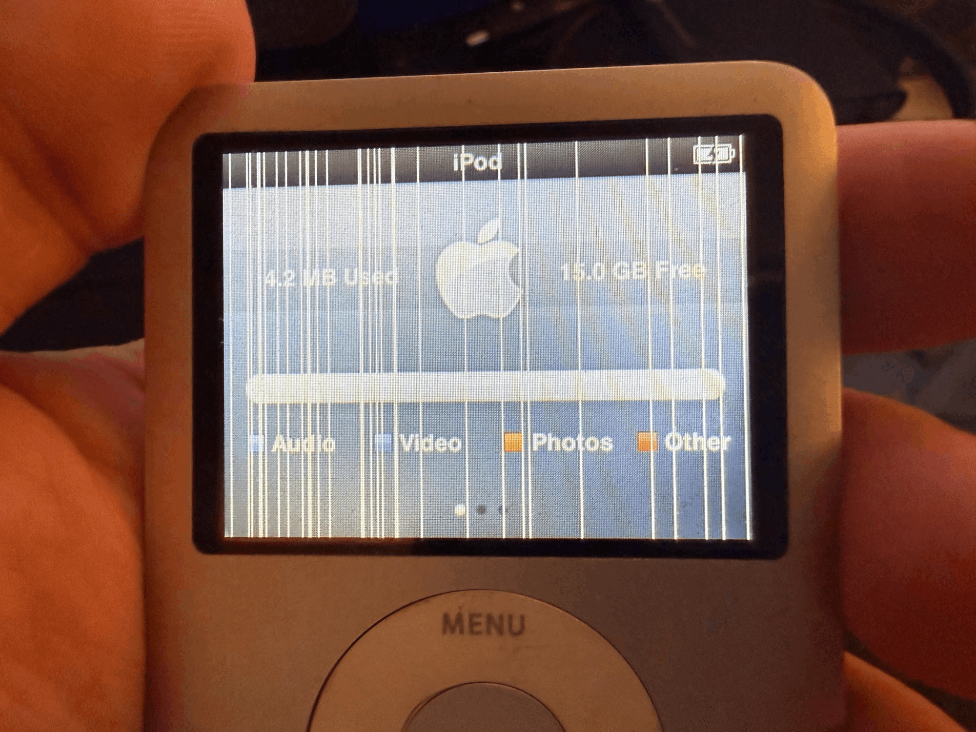
But there's one more problem I had to face: it was a bit unstable.
Power and Partition Problems
Once RetailOS was stable enough to actually use, a new problem showed up: the iPod worked, and then it stopped working. After a bit of use (syncing, poking around, etc.) I'd be greeted by bdsw - the "restore with iTunes" screen - and it turns out that it was two different problems. Easy to fix problems, mercifully.
Syncing music through iTunes didn't kill the iPod during the transfer which was good to see, but it died when I ejected it, soon after the "OK to Disconnect" screen was done indexing (or, sometimes, during it). When it came back, it gave me bdsw which said to me that something was probably corrupting the filesystem partition so bad that it was unable to load osos subsequently. Syncing something as little as five songs all the way to syncing thirteen gigabytes caused the failure in exactly the same way. Fixing it was as simple as recovering it again (even just the firmware step, skipping WTF and replacing the NOR contents), but that meant losing everything in the data partition because it would rewrite the table.
The actual root cause was the battery. It's degraded, and USB alone can't carry the current the NAND stack draws during a program/erase burst. With a bench supply on the battery leads, it certainly got more stable. The iPod survived more reboots, but still wasn't exceedingly stable. After some use, bdsw would come back. And also games wouldn't launch. That's… odd. If the FTL is intact then nothing above it should be complaining about it, right?
The device sat in bdsw, so I did the boring thing and dumped the disk from disk mode. The partition table had one entry: a FAT32 partition. There was no firmware partition entry at all. The firmware volume - the MSE container with rsrc, osos, and aupd in it - lives at LBA 63 and runs 128MiB, to LBA 32830. The FAT32 data partition started at LBA 256 and ran to the end of the chip. The overlap was 99.4% of the firmware volume.
Once again, the problem was me all along. I was using gparted to format the disk. Make an msdos partition table, make a FAT32 partition, let the iPod create its system folders, sync with iTunes, life goes on. But that turns out to be the wrong thing to do. Restore writes the firmware volume, then a repartition step zeroes the front of the disk and drops the firmware entry, then iTunes fills the FAT32 filesystem from LBA 256 upward - directly over the boot image. The rsrc partition goes first, so games break before boot does. Then the directory goes, then osos, and the EFI's boot chain fails, and you get bdsw. Filling the iPod with music is the mechanism that destroys it.
My tool should be the one authoring the partition table, not gparted after the fact. In fact, my tool doesn't write the table, it tells the iPod to write the table. There's a repartition command that exists on the device and is correct, but nothing in my restore path ever called it. Partitioning was a manual step in my workflow, and the hand-run mkfs.fat left its signature sitting at LBA 256 as a confession.
Once it repartitions, it reads the table back and re-reads the MSE directory from the device, requiring rsrc and osos to be present before it calls the restore complete. The data partition now starts at LBA 32831 - one block past the end of the firmware volume. You still need to use something like mkfs.fat but under no circumstances should you make your own partition table.
Complete!
Once the power and partition problems were solved, I was able to use the "fill free space with music" option in iTunes and load the iPod completely with music and have it survive. I was also able to put a bunch of movies on it - I transcoded and uploaded all of the Harry Potter movies and had a bunch of music on there. Pretty neat!
Finally, this iPod completely works and has 16GB worth of data on there. A long on-again-off-again project that has lasted longer than my real-life relationship finally comes to a close. I've messed with iPod memory, iPod Bluetooth, iPad screens… I think I might leave behind modding Apple products for now and focus on other things. I have some ideas, but I don't want to become a 100% tech-project channel. Either way, I'm very proud of this.
All of the code for this project is available on GitHub: lemonjesus/iPod-n3g-16gb.
Disclosure of AI Use
I believe if AI is used on a project in some meaningful way, it should be disclosed. Given this project has been running for longer than vibe-coding has been around, these disclosures really only apply to the last few months of progress where it helped me get over a few humps that otherwise would have taken me months and more burnouts. I have overarching principles on my personal use of AI that you can read about here, but for this project specifically:
- No part of this was shipped without me reading and understanding it. Every line of code and documentation is either written by me or is something I approved to be written. I've reviewed every line either I or an LLM has written.
- Various LLMs were used to help me understand patterns in firmware that I had never seen before and help me make sense of it. Increasingly important as I got deeper into the software stack (the deeper you get, the more tangled the binaries become, and it was nice to have that help).
- All but one patch category was discovered/piloted or written by me. The patch category an LLM (in this case, Claude) discovered that I can't take credit for: the ECC Scrubbing Patches.
- This writeup and the accompanying YouTube video's script were 100% written by me.
Acknowledgments
When this project started, tooling was sparse, the community scattered, and overall everything was very "ten years ago." Now, there's amazing tooling and a thriving community working on iPod Nano stuff. The ones that were specifically useful to this project:
- q3k's wInd3x - not only is this exploit/tool/etc. what my patcher is based on, but it's also what replaced tracking EFI patches with spreadsheets (because the madman wrote an EFI modification engine into it).
- slackware - was one of my first points of contact and helped me get started with the software research side of things. He's also incredibly active in the community and manages freemyipod.org and the associated GitHub projects (where wInd3x and QEMU and Linux for the iPod reside).
- benedikt93 and Cástor Muñoz - laid a lot of groundwork for reverse engineering the NAND stuff. Also, Castor wrote the Rockbox bootloader for the n3g which was the only way I had to work with the device at the beginning. Very grateful their work wasn't lost to the sands of time.
- Countless others from the Discord community who have contributed to the zeitgeist of iPod Nano modding. We've cultivated a lovely community, and you should pop in and learn more and contribute if you made it all the way to the end of this writeup!